🔌Intro to Electrical Engineering Unit 15 Review
15.1 Design and analysis of combinational circuits
15.1 Design and analysis of combinational circuits
Unit & Topic Study Guides
Intro to Electrical Engineering
Electrical Quantities and Units
Ohm's Law: Understanding Resistance
Kirchhoff's Laws in Electrical Engineering
Circuit Analysis Techniques
Capacitance and Inductance
Transient Response: First-Order Circuits
Steady-State Sinusoidal Analysis
Semiconductor Basics in Electrical Engineering
Diodes and Circuits
BJTs: Bipolar Junction Transistors
Field-Effect Transistors in Electronics
Digital Systems Fundamentals
Boolean Algebra & Logic Gates
Combinational Logic Circuits
Sequential Logic Circuits
Signal Processing Fundamentals
Continuous-Time Signals & Systems
Fourier Series and Transforms
Sampling and Discrete-Time Signals
Z-Transforms in Discrete-Time Systems
Circuit Simulation Tools Overview
System Modeling & Analysis Tools
Case Studies in Electrical Engineering
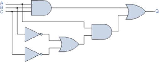
Combinational logic circuits are the building blocks of digital systems. They take binary inputs, process them through logic gates, and produce outputs based solely on the current inputs. There's no memory involved, no feedback loops. What goes in right now determines what comes out right now.
To design these circuits well, you need Boolean algebra to describe and simplify logic, Karnaugh maps to optimize gate count, and an understanding of timing and loading effects (propagation delay, fan-in, fan-out) to make sure your circuit actually works at speed.
Boolean Algebra and Logic
Fundamentals of Boolean Algebra
Boolean algebra is the math behind digital logic. It works with just two values, 0 and 1, and three core operations: AND, OR, and NOT. Every combinational circuit you'll ever build can be described by a Boolean expression using these operations.
Boolean expressions follow a set of laws that let you rearrange and simplify them:
- Commutative: and
- Associative:
- Distributive:
These aren't just abstract rules. You'll use them constantly to reduce a messy expression into something you can actually build with fewer gates.
Truth tables are the other essential tool here. A truth table lists every possible combination of inputs and shows the corresponding output. For inputs, you get rows. If you have 3 inputs, that's 8 rows. The truth table is often your starting point: you define what the circuit should do, then use Boolean algebra (or K-maps) to figure out how to build it.
Logic Gates and Combinational Logic
Logic gates are the physical components that implement Boolean operations. Each gate type has a defined truth table:
- AND: output is 1 only when all inputs are 1
- OR: output is 1 when at least one input is 1
- NOT (inverter): flips the input (0 becomes 1, 1 becomes 0)
- NAND: opposite of AND (output is 0 only when all inputs are 1)
- NOR: opposite of OR (output is 0 only when at least one input is 1)
- XOR: output is 1 when inputs differ
- XNOR: output is 1 when inputs are the same
NAND and NOR are especially important because each one is functionally complete. That means you can build any logic function using only NAND gates or only NOR gates. This matters in real chip design where manufacturing with a single gate type simplifies fabrication.
Combinational circuits connect these gates together to perform more complex tasks. Common examples include:
- Adders (half-adder, full-adder): perform binary addition
- Decoders: convert an -bit input into one of output lines
- Multiplexers (MUX): select one of several inputs to pass to the output based on select lines
- Comparators: determine whether two binary values are equal, or which is greater
The defining feature of all these circuits is that the output depends only on the present inputs.

Circuit Optimization
Karnaugh Maps and Minimization Techniques
A Karnaugh map (K-map) is a visual method for simplifying Boolean expressions. Instead of grinding through algebraic manipulations, you plot the truth table onto a grid and look for patterns.
Here's the process for using a K-map:
- Start with the truth table for your function.
- Draw the K-map grid. For a 2-variable function it's a 2×2 grid; for 3 variables, 2×4; for 4 variables, 4×4. Label the rows and columns using Gray code ordering (so adjacent cells differ by only one variable).
- Fill in each cell with the output value (0 or 1) from the truth table.
- Group adjacent 1s into rectangular groups. Groups must be powers of 2 in size (1, 2, 4, 8, etc.). Larger groups give simpler terms.
- The K-map wraps around: the leftmost column is adjacent to the rightmost, and the top row is adjacent to the bottom.
- Write the simplified product term for each group by identifying which variables stay constant across the group.
- OR all the product terms together to get the minimized SOP expression.
Why bother? Minimization reduces the number of gates you need, which lowers power consumption, reduces chip area, and can improve speed. For functions with more than 4 or 5 variables, algorithmic methods like the Quine-McCluskey algorithm are used instead, since K-maps become impractical to draw.
Canonical Forms and Standard Representations
Canonical forms give you a standardized way to write any Boolean function. The two main forms are:
- Sum of Products (SOP): the function is written as an OR of AND terms. Each AND term (called a minterm) corresponds to exactly one row of the truth table where the output is 1. For example, is an SOP expression.
- Product of Sums (POS): the function is written as an AND of OR terms. Each OR term (called a maxterm) corresponds to a row where the output is 0.
SOP is more commonly used as a starting point because it maps directly from the 1s in a truth table. You can convert between SOP and POS using De Morgan's laws:
Canonical forms are useful because they give you a consistent starting point before you apply minimization. Two functions that look different as arbitrary expressions will look identical once you write them in the same canonical form, making comparison straightforward.
Circuit Performance
Propagation Delay and Timing Analysis
Propagation delay () is the time between when an input changes and when the output settles to its new value. Every real gate has some delay, typically measured in nanoseconds. A NOT gate might have a of 1-2 ns, while a more complex gate could be slower.
When gates are chained together, their delays add up along each path through the circuit. The critical path is the longest delay path from any input to any output. This path determines how fast the entire circuit can operate.
To find the critical path:
- Identify all paths from inputs to outputs.
- Add up the propagation delays of every gate along each path.
- The path with the largest total delay is the critical path.
The critical path delay sets the minimum clock period for any synchronous system using that combinational block. If your critical path delay is 10 ns, the circuit can't be clocked faster than .
This is why minimization matters for performance, not just gate count. Fewer gates in series means a shorter critical path and a faster circuit.
Fan-In and Fan-Out Considerations
Fan-in is the number of inputs a gate accepts. A 2-input AND gate has a fan-in of 2; an 8-input AND gate has a fan-in of 8. Higher fan-in means each input has to charge more internal capacitance, which increases the gate's propagation delay. If you need a large AND function, it's often faster to cascade smaller gates (e.g., two 4-input ANDs feeding a 2-input AND) rather than using a single high-fan-in gate.
Fan-out is the number of gate inputs that a single output drives. If one gate's output connects to the inputs of 5 other gates, its fan-out is 5. Each load adds capacitance that the driving gate must charge and discharge, so higher fan-out means slower transitions and more delay.
Practical guidelines for managing fan-in and fan-out:
- Check the datasheet for maximum rated fan-out. Exceeding it can cause the output voltage to fall outside valid logic levels, leading to unreliable behavior.
- Insert buffers or drivers when a signal needs to reach many gates. The buffer restores signal strength and keeps the fan-out of the original gate manageable.
- For high-fan-in functions, break them into a tree structure of smaller gates to balance delay.
- Proper transistor sizing in custom designs helps optimize both fan-in and fan-out characteristics.
Getting fan-in and fan-out right is the difference between a circuit that works on paper and one that works on a chip.