🔌Intro to Electrical Engineering Unit 11 Review
11.1 BJT structure and operation
11.1 BJT structure and operation
Unit & Topic Study Guides
Intro to Electrical Engineering
Electrical Quantities and Units
Ohm's Law: Understanding Resistance
Kirchhoff's Laws in Electrical Engineering
Circuit Analysis Techniques
Capacitance and Inductance
Transient Response: First-Order Circuits
Steady-State Sinusoidal Analysis
Semiconductor Basics in Electrical Engineering
Diodes and Circuits
BJTs: Bipolar Junction Transistors
Field-Effect Transistors in Electronics
Digital Systems Fundamentals
Boolean Algebra & Logic Gates
Combinational Logic Circuits
Sequential Logic Circuits
Signal Processing Fundamentals
Continuous-Time Signals & Systems
Fourier Series and Transforms
Sampling and Discrete-Time Signals
Z-Transforms in Discrete-Time Systems
Circuit Simulation Tools Overview
System Modeling & Analysis Tools
Case Studies in Electrical Engineering
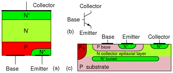
BJT Structure
A BJT is a three-layer semiconductor device built to amplify electrical signals or act as a switch. Understanding how those three layers interact is the foundation for everything else you'll learn about transistor circuits.
Semiconductor Layers
A BJT has three regions, each with a specific job:
- Emitter: Heavily doped so it can inject a large number of charge carriers (electrons in NPN, holes in PNP) into the base. The heavy doping is what makes the emitter the "source" of carriers.
- Base: A very thin, lightly doped layer sandwiched in the middle. Because it's thin, most carriers that enter from the emitter can pass straight through without recombining. Because it's lightly doped, it doesn't contribute many carriers of its own. The base is what gives you control over the transistor.
- Collector: Moderately doped and physically the largest region. Its job is to collect the carriers that make it through the base. The collector-base junction is typically reverse-biased during normal amplification, which creates an electric field that sweeps carriers across.
The doping concentrations follow a deliberate order: emitter is the most heavily doped, then collector, then base. Getting these ratios right is what makes the transistor work efficiently.
Transistor Types
There are two types of BJTs:
- NPN: A thin p-type base sits between an n-type emitter and an n-type collector. Current carriers are electrons, which have higher mobility than holes. This makes NPN transistors faster and more efficient, which is why they're more common in practice.
- PNP: A thin n-type base sits between a p-type emitter and a p-type collector. Current carriers are holes. PNP transistors work on the same principles but with reversed voltage polarities and current directions.
A quick way to remember: in an NPN transistor, conventional current flows into the collector and out of the emitter. In a PNP, it's the opposite.
BJT Operation Modes
BJTs have three main operating modes, determined by how the two junctions (base-emitter and base-collector) are biased.
Forward-Active Mode
This is the mode used for amplification. Here's what's happening step by step:
- The base-emitter (BE) junction is forward-biased, which lowers the barrier and allows the emitter to inject carriers into the base.
- Because the base is very thin and lightly doped, most of these carriers (say, electrons in an NPN) diffuse across the base without recombining.
- The base-collector (BC) junction is reverse-biased, creating a strong electric field in the depletion region that sweeps those carriers into the collector.
- A small base current controls a much larger collector current , giving you amplification.
The relationship is:
where is the current gain. Only a tiny fraction of the carriers recombine in the base, which is why the base current is so small compared to the collector current.
Saturation and Cutoff Modes
These two modes are used when the transistor acts as a switch (common in digital logic).
- Saturation: Both the BE and BC junctions are forward-biased. The transistor is fully "on," acting like a closed switch with a small voltage drop between collector and emitter (typically around 0.2–0.3 V). Increasing the base current further doesn't significantly increase because the transistor is already fully conducting.
- Cutoff: Both junctions are reverse-biased (or at least the BE junction is below its turn-on voltage). The transistor is fully "off," acting like an open switch. Collector current is essentially zero, and nearly the full supply voltage appears across the collector-emitter terminals.
In digital circuits, saturation represents a logic LOW at the collector (low voltage), and cutoff represents a logic HIGH (high voltage). That's how BJTs implement basic switching and logic.
BJT Parameters
Current Gain ()
The current gain (also called ) tells you how effectively the transistor amplifies:
Typical values range from about 50 to 200 for common transistors, though some can be higher. A of 100 means that for every 1 mA of base current, you get roughly 100 mA of collector current.
A few things to keep in mind about :
- It's not a fixed constant. It varies with temperature, collector current level, and even from one transistor to another of the same part number.
- Because is unreliable, practical circuit designs usually don't depend on its exact value. You'll learn biasing techniques later that make circuits work across a wide range of .
Emitter Injection Efficiency
Emitter injection efficiency measures how much of the emitter current actually consists of the "useful" carriers being injected into the base (as opposed to carriers flowing the wrong way across the junction).
For an NPN transistor:
where is the electron current injected from the emitter into the base, and is the total emitter current.
You want as close to 1 as possible. Modern transistors achieve values of 0.95 to 0.99. The main way to push higher is to dope the emitter much more heavily than the base, which ensures that the vast majority of current across the BE junction comes from emitter-to-base carrier injection rather than base-to-emitter flow.