🧗♀️Semiconductor Physics Unit 4 Review
4.2 Shockley-Read-Hall recombination
4.2 Shockley-Read-Hall recombination
Unit & Topic Study Guides
Semiconductor Materials and Crystal Structure
Energy Bands & Carrier Transport in Semiconductors
Equilibrium Carrier Statistics in Semiconductors
Excess Carriers & Recombination-Generation
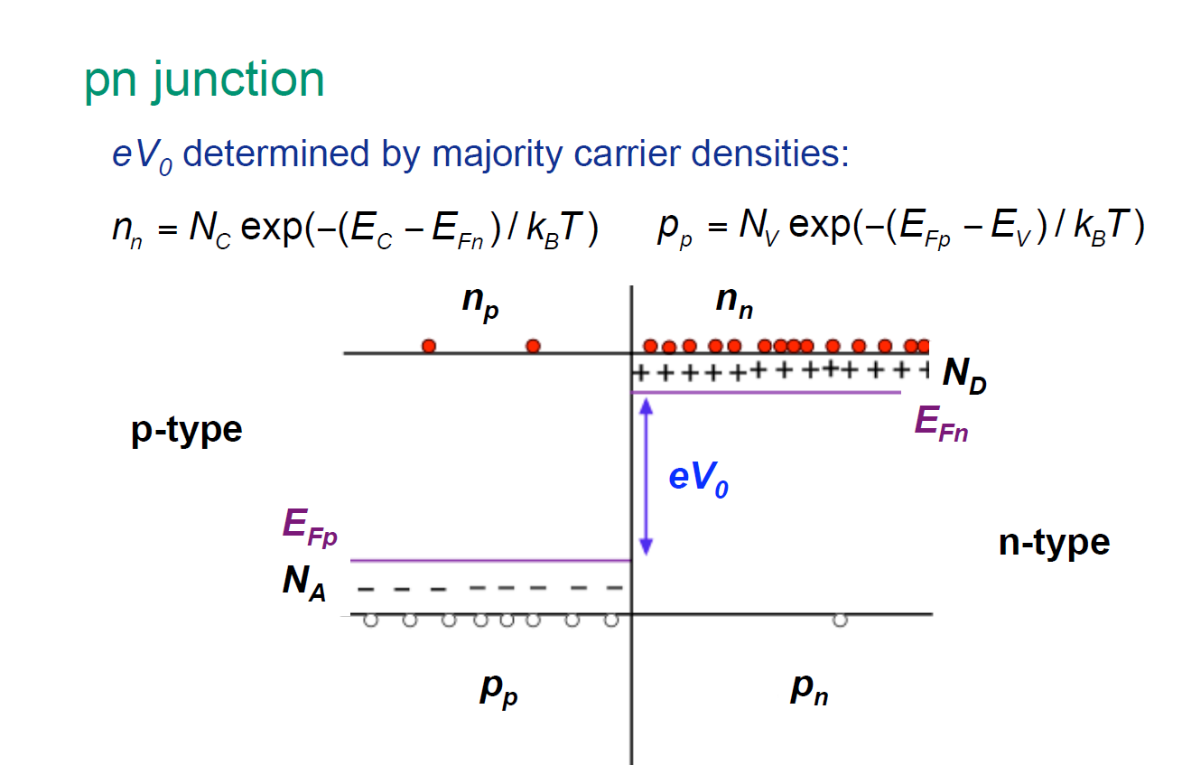
P-N Junctions in Semiconductor Devices
Metal-Semiconductor Junctions
MOS Capacitors in Semiconductor Physics
MOSFETs: Semiconductor Field-Effect Devices
BJTs: Principles and Applications
Optoelectronic Devices in Semiconductor Physics
Power Semiconductor Devices
Shockley-Read-Hall Recombination
Shockley-Read-Hall (SRH) recombination is the dominant recombination mechanism in most practical semiconductors. Electrons and holes recombine not by direct band-to-band transitions, but through intermediate trap states introduced by defects or impurities in the crystal lattice. Because this process is non-radiative, the recombination energy dissipates as heat (phonons) rather than light.
SRH recombination directly limits the performance of solar cells, LEDs, and transistors by reducing carrier lifetimes and increasing leakage currents. Controlling it through material purity and passivation is one of the central challenges in device engineering.
Recombination vs Generation
Recombination and generation are opposing processes that together govern carrier populations:
- Recombination: an electron in the conduction band transitions to the valence band and annihilates a hole, reducing the carrier count.
- Generation: an electron is excited from the valence band to the conduction band, creating a new electron-hole pair.
Under thermal equilibrium, these two processes balance exactly, so the net recombination rate is zero. When excess carriers are injected (by light or bias), recombination exceeds generation until equilibrium is restored.
Recombination Through Defect Levels
Defects, dislocations, or impurity atoms in the crystal introduce allowed energy levels inside the bandgap. These are called trap states (or deep levels). A trap state acts as a stepping stone: it can capture an electron from the conduction band and then capture a hole from the valence band (or vice versa), completing a recombination event in two steps rather than one.
This two-step process is far more probable than a direct band-to-band transition in indirect-gap materials like silicon, which is why SRH recombination dominates there.
Carrier Capture and Emission
Each trap can undergo four elementary processes:
- Electron capture: a conduction-band electron falls into the empty trap.
- Electron emission: a trapped electron is thermally excited back into the conduction band.
- Hole capture: a valence-band hole is captured by the occupied trap (equivalently, the trapped electron falls to the valence band).
- Hole emission: a hole is emitted from the trap back into the valence band (equivalently, a valence-band electron is excited into the trap).
The rates of capture depend on the carrier concentration, the capture cross-section of the trap, and the thermal velocity of the carriers. Emission rates depend on the trap energy relative to the band edges and on temperature.
Capture Cross-Sections
The capture cross-section ( for electrons, for holes) quantifies how "large" a trap appears to a passing carrier. It has units of area (typically ) and depends on the physical and electronic nature of the defect.
- Coulombic-attractive traps (e.g., a positively charged defect capturing an electron) tend to have large cross-sections, on the order of to .
- Neutral traps are smaller, around to .
- Coulombic-repulsive traps have the smallest cross-sections.
Larger capture cross-sections mean faster capture, higher recombination rates, and shorter carrier lifetimes.
Thermal Velocity of Carriers
The thermal velocity is the average speed of a carrier due to random thermal motion:
where is Boltzmann's constant, is the absolute temperature, and is the carrier effective mass. At 300 K in silicon, is roughly . Higher thermal velocity increases the rate at which carriers encounter traps, raising the capture rate.
The SRH Recombination Rate
The net SRH recombination rate per unit volume is:
where:
- , are the electron and hole concentrations
- is the intrinsic carrier concentration
- and are the electron and hole capture time constants ( is the trap density)
- and are the carrier concentrations that would exist if the Fermi level sat at the trap energy
The numerator tells you the driving force: recombination is positive when the carrier product exceeds the equilibrium value, and the rate goes to zero at thermal equilibrium where .
Derivation Outline
The SRH rate equation comes from balancing the four capture/emission processes at steady state:
- Write the rate of electron capture into the trap and the rate of electron emission out of the trap.
- Write the analogous rates for hole capture and hole emission.
- At steady state, the net electron flow into the trap equals the net hole flow into the trap (the trap occupation isn't changing).
- Apply the detailed balance principle: at equilibrium each process individually balances its reverse, which lets you express emission rates in terms of capture rates and , .
- Solve for the trap occupation fraction and substitute back to get .
Trap Energy Level Effects
The position of the trap in the bandgap has a huge effect on recombination efficiency:
- Mid-gap traps () are the most effective recombination centers. At mid-gap, , which minimizes the denominator of the SRH rate expression and maximizes .
- Shallow traps ( near a band edge) are poor recombination centers. A trap close to the conduction band captures electrons easily but re-emits them before a hole can be captured. It acts more as a temporary trapping center than a recombination center.
This is why contaminants like gold and copper in silicon (which introduce mid-gap levels) are so damaging to carrier lifetime, while shallow dopants like phosphorus and boron are not.
Minority and Majority Carrier Traps
Whether a trap preferentially captures minority or majority carriers depends on the ratio and the trap energy:
- A minority carrier trap captures minority carriers more readily. These traps strongly influence the recombination rate because minority carriers are the bottleneck.
- A majority carrier trap captures majority carriers first. Its impact on recombination depends on whether it can subsequently capture a minority carrier before re-emitting the majority carrier.
The distinction matters most at low injection, where the minority carrier supply limits recombination.

Electron and Hole Lifetimes
- Electron lifetime : the average time a conduction-band electron survives before being captured by a trap.
- Hole lifetime : the average time a valence-band hole survives before being captured.
Both are inversely proportional to the trap density , the capture cross-section, and the thermal velocity:
Cleaner material (lower ) gives longer lifetimes. This is why high-purity float-zone silicon has lifetimes of milliseconds, while heavily contaminated Czochralski silicon may have lifetimes of only microseconds.
Minority Carrier Lifetime
In most device contexts, the minority carrier lifetime is the parameter that matters. In p-type material, electrons are the minority carriers, and their lifetime governs how long photogenerated electrons survive before recombining. In n-type material, the hole lifetime plays that role.
Longer minority carrier lifetimes translate directly to better device performance: higher open-circuit voltage in solar cells, higher current gain in bipolar transistors, and better sensitivity in photodetectors.
Carrier Diffusion Length
The diffusion length is the average distance a carrier diffuses before recombining:
where is the diffusion coefficient and is the carrier lifetime. For electrons in p-type silicon with and , the diffusion length is about 170 . Carriers generated farther than roughly one diffusion length from a collecting junction are likely to recombine before being collected.
Injection Level Dependence
The injection level is the ratio of excess carrier concentration to the equilibrium majority carrier concentration.
- Low injection ( or ): the recombination rate simplifies to . The lifetime is constant and determined by the minority carrier capture time.
- High injection (): both carrier types are present in comparable concentrations, and the effective lifetime approaches . The recombination rate becomes less sensitive to trap energy.
The transition between these regimes occurs when becomes comparable to the doping concentration.
Steady-State Conditions
Under steady-state conditions, the generation rate exactly balances the recombination rate, so carrier concentrations don't change with time. This is the standard assumption in most device analyses (e.g., calculating the I-V curve of a solar cell under constant illumination). Time-dependent problems, like turn-on transients, require solving the full continuity equations.
Quasi-Fermi Levels
When a semiconductor is driven out of equilibrium (by light or applied voltage), a single Fermi level no longer describes the carrier populations. Instead, you define:
- : the electron quasi-Fermi level, describing the electron population
- : the hole quasi-Fermi level, describing the hole population
The product . When , and net recombination occurs. The quasi-Fermi level splitting is a direct measure of how far the system is from equilibrium.
Temperature Dependence
SRH recombination rates generally increase with temperature for two reasons:
- The thermal velocity increases, raising capture rates.
- The intrinsic carrier concentration increases exponentially with temperature, which affects the equilibrium term and the parameters and .
At elevated temperatures, increased thermal emission from traps can also change the effective trap occupation, complicating the picture.
Doping Concentration Effects
Higher doping affects SRH recombination in several ways:
- It shifts the Fermi level toward a band edge, changing the equilibrium occupation of traps.
- It increases the majority carrier concentration, which can speed up one of the two capture steps.
- Heavy doping can introduce additional crystal damage and defects, increasing .
- At very high doping (), bandgap narrowing and Auger recombination often become more important than SRH.
Surface vs Bulk Recombination
- Bulk recombination occurs throughout the volume of the semiconductor, governed by the bulk trap density.
- Surface recombination occurs at surfaces and interfaces where the crystal terminates. Dangling bonds and interface states create a high density of traps, making surfaces potent recombination sites.
Surface recombination is characterized by a surface recombination velocity (units of cm/s). Typical unpassivated silicon surfaces have , while well-passivated surfaces (e.g., with thermal ) can achieve . Passivation techniques (oxide growth, hydrogen termination, dielectric coatings) are critical for high-efficiency devices.
Radiative vs Non-Radiative Recombination
- Radiative recombination: the electron-hole pair recombines by emitting a photon. This is the desired process in LEDs and lasers.
- Non-radiative recombination (including SRH): the recombination energy is released as phonons (heat). This is a loss mechanism in all devices.
In direct bandgap semiconductors like GaAs, radiative recombination is efficient because the transition conserves crystal momentum. In indirect bandgap semiconductors like Si, a phonon must assist the transition, making radiative recombination slow and SRH recombination the dominant pathway.
Direct and Indirect Bandgap Semiconductors
- Direct bandgap: the conduction band minimum and valence band maximum occur at the same crystal momentum (-value). Examples: GaAs, InP, GaN.
- Indirect bandgap: the conduction band minimum and valence band maximum are at different -values. Examples: Si, Ge.
Because SRH recombination doesn't require momentum conservation (the trap provides a localized state), it operates efficiently in both types. But its relative importance is much greater in indirect-gap materials, where the competing radiative channel is weak.
Auger Recombination Comparison
Auger recombination is another non-radiative mechanism, but it involves three carriers: an electron and hole recombine, and the released energy is transferred to a third carrier (which then thermalizes).
| Feature | SRH | Auger |
|---|---|---|
| Carriers involved | 2 (via trap) | 3 |
| Rate dependence | Linear in (low injection) | Goes as or |
| Dominant regime | Low-to-moderate injection, defective material | High injection, high doping |
| Defect dependence | Strong (proportional to ) | Intrinsic to the material |
In high-purity, lightly doped silicon at low injection, SRH dominates. At very high doping or high injection (e.g., the emitter of a solar cell), Auger takes over.
Assumptions and Limitations of the SRH Model
The standard SRH model makes several simplifying assumptions:
- A single trap level with fixed energy (real materials often have a distribution of trap levels).
- Capture cross-sections are constant, independent of trap occupancy and electric field.
- Trap density is spatially uniform.
- Capture and emission processes are independent of other recombination mechanisms.
These assumptions work well for dilute, well-characterized defects but break down for heavily defected regions, interfaces with continuous distributions of states, or high-field regions where field-enhanced emission (Poole-Frenkel effect) becomes significant.
Device Performance Impact
SRH recombination affects nearly every semiconductor device:
- Solar cells: recombination of photogenerated carriers through traps reduces the short-circuit current and open-circuit voltage, directly lowering power conversion efficiency.
- LEDs: SRH competes with radiative recombination, reducing the internal quantum efficiency. This is especially problematic at low current densities where SRH can dominate.
- Bipolar transistors: recombination in the base region reduces the current gain and slows switching.
Leakage Current and Dark Current
In a reverse-biased p-n junction, the depletion region has , so SRH traps act as generation centers rather than recombination centers. This thermal generation of carriers produces a leakage (dark) current that flows even without illumination or forward bias.
The generation current is proportional to (where is the generation lifetime), so it increases strongly with temperature. This is a major concern for photodetectors and image sensors, where dark current sets the noise floor.
Solar Cell Efficiency Limitations
SRH recombination is one of the primary loss mechanisms in crystalline silicon solar cells. Reducing it requires:
- Using high-purity silicon with low bulk trap density
- Applying surface passivation to minimize surface recombination
- Optimizing processing steps to avoid introducing metallic contaminants
Record-efficiency silicon cells achieve bulk lifetimes exceeding 10 ms through careful control of these factors.
LED Efficiency Droop
At high drive currents, LED efficiency decreases, a phenomenon called efficiency droop. While Auger recombination is considered the primary cause in GaN-based LEDs, SRH recombination contributes at low current densities where the carrier concentration in the active region is still modest. The interplay between SRH (dominant at low current), radiative (dominant at moderate current), and Auger (dominant at high current) recombination shapes the entire efficiency-vs-current curve.
Experimental Characterization Techniques
Several techniques are used to measure SRH-related parameters:
- Deep Level Transient Spectroscopy (DLTS): measures the capacitance transient of a junction device after a filling pulse. By varying the temperature, you can extract the trap energy level, capture cross-section, and density.
- Photoluminescence (PL): the intensity and spectrum of light emitted under optical excitation reveal the balance between radiative and non-radiative recombination. Lower PL intensity (relative to a reference) indicates stronger non-radiative losses.
- Time-resolved PL (TRPL): measures the decay of PL intensity after a short laser pulse. The decay time constant gives the effective carrier lifetime.
- Transient absorption spectroscopy: monitors changes in optical absorption after pulsed excitation, tracking carrier populations directly.
Carrier Lifetime Extraction Methods
Extracting carrier lifetimes from measurements:
- TRPL decay fitting: fit the PL decay curve to a single or multi-exponential function. The dominant time constant is the effective lifetime.
- Open-circuit voltage decay (OCVD): illuminate a solar cell to steady state, then switch off the light and record the voltage decay. The slope of vs. time gives the minority carrier lifetime via .
- Photoconductivity decay (PCD): measure the decay of photoconductivity (via microwave reflection or contactless methods) after a light pulse. The decay time constant equals the effective lifetime.
- Quasi-steady-state photoconductance (QSSPC): a widely used technique in the solar cell industry where a slowly decaying flash illuminates the sample and the photoconductance is measured continuously, yielding lifetime as a function of injection level.