The free electron model simplifies how electrons behave in metals by treating conduction electrons as a gas of non-interacting particles moving freely through the material. This is the starting point for electronic band theory: it gives you a tractable framework that already explains electrical conductivity, thermal properties, and basic optical behavior in simple metals. Where it breaks down (band gaps, magnetism, strong correlations) points directly toward the more sophisticated models you'll encounter later in this unit.
Free electron model basics
The core idea is straightforward: ignore the ions, ignore other electrons, and ask what happens when electrons roam freely inside a box the size of your sample. Despite these drastic simplifications, the model captures a surprising amount of real metal physics.
Assumptions and limitations
- Electrons move freely with no interaction with the ionic lattice (the potential inside the metal is treated as flat)
- Electron-electron interactions are neglected; each electron is treated as independent
- The periodic potential of the crystal structure is completely ignored
- Works well for alkali metals (sodium, potassium) where the single valence electron is loosely bound and the Fermi surface is nearly spherical
- Fails for transition metals, where d-electron bonding and complex Fermi surfaces matter
- Cannot explain band gaps in semiconductors or insulators, since there's no periodic potential to open gaps
Drude model vs Sommerfeld model
These are two versions of the free electron model, separated by whether you use classical or quantum statistics.
Drude model (classical):
- Treats electrons as a classical ideal gas obeying Maxwell-Boltzmann statistics
- Successfully derives expressions for electrical and thermal conductivity
- Predicts electronic specific heat of per electron, which is far too large compared to experiment. Measured electronic specific heat in metals is roughly 100 times smaller at room temperature.
Sommerfeld model (quantum):
- Replaces Maxwell-Boltzmann with Fermi-Dirac statistics, recognizing that electrons are fermions
- Only electrons within of the Fermi energy can be thermally excited, which explains why the electronic specific heat is so small: , linear in
- Correctly accounts for the Wiedemann-Franz law relating thermal and electrical conductivity
Both models share the assumptions of constant electron density and isotropic (scalar) effective mass.
Quantum mechanical approach
Treating electrons quantum mechanically means solving the Schrödinger equation for particles in a box. The solutions are plane waves with quantized wavevectors, and the Pauli exclusion principle forces electrons to fill states from the bottom up. This single change from classical to quantum statistics resolves the specific heat problem and explains Pauli paramagnetism.
Fermi-Dirac distribution
Because electrons are fermions, no two can occupy the same quantum state. The probability that a state at energy is occupied at temperature is:
At , this is a sharp step function: all states below are filled, all above are empty. At finite temperature, the step smears out over a window of width around . Since for typical metals at room temperature ( eV vs eV), only a tiny fraction of electrons near the Fermi level participate in thermal processes.
Density of states
The density of states counts how many electronic states exist per unit energy per unit volume. For free electrons in 3D:
The dependence is specific to three dimensions. In 2D, is constant; in 1D, it goes as . The density of states at the Fermi level, , directly controls the electronic specific heat, Pauli susceptibility, and tunneling rates.
Electronic properties
Electrical conductivity
From the Drude framework, applying Newton's second law to electrons experiencing an electric field and scattering events with average relaxation time :
Here is the conduction electron density, is the electron charge, and is the electron mass. In metals, is roughly temperature-independent, so the temperature dependence of comes from . At high temperatures, phonon scattering dominates and decreases (resistance increases linearly with ). At low temperatures, impurity scattering sets a residual resistivity floor.
Thermal conductivity
Electrons carry heat as well as charge. The Wiedemann-Franz law connects the two:
where is the Lorenz number:
This explains why good electrical conductors (copper, silver) are also good thermal conductors. Significant deviations from this law at intermediate temperatures signal that elastic scattering assumptions are breaking down or that electron-electron scattering is important.
Hall effect
When a magnetic field is applied perpendicular to a current-carrying sample, the Lorentz force deflects carriers sideways, building up a transverse Hall voltage. The Hall coefficient for free electrons is:
The sign of tells you the carrier type: negative for electrons, positive for holes. Measuring gives you the carrier concentration directly. Some metals (beryllium, aluminum) show a positive Hall coefficient, which the free electron model cannot explain. This is one of the clearest signals that band structure effects matter.
Band structure
Nearly free electron model
This is the natural next step beyond the free electron model. You keep the free electron picture but add a weak periodic potential representing the ion cores. The key result: wherever a free-electron energy parabola would cross a Brillouin zone boundary, the periodic potential opens an energy gap. States just below the gap are pushed down in energy; states just above are pushed up.
The size of the gap is proportional to the Fourier component of the periodic potential at that reciprocal lattice vector: . This explains why some materials are metals (Fermi level sits within a band) and others are insulators (Fermi level falls inside a gap).
Brillouin zones
Brillouin zones are the Wigner-Seitz cells of the reciprocal lattice in -space. They organize the allowed electron wavevectors:
- The first Brillouin zone contains all unique electronic states; everything outside can be folded back in using reciprocal lattice vectors
- Zone boundaries are where Bragg reflection occurs, and energy gaps open in the nearly free electron model
- The shape of the Brillouin zone depends on the crystal structure (BCC, FCC, etc.) and directly affects which states are near the Fermi level
Fermi surface
The Fermi surface is the constant-energy surface in -space at . For free electrons it's a perfect sphere. In real metals, the periodic potential distorts it, sometimes dramatically. The geometry of the Fermi surface controls transport properties, because only electrons near this surface respond to external fields.
Fermi energy and wavevector
At , electrons fill states up to the Fermi energy:
The corresponding Fermi wavevector is:
Note that depends only on the electron density. For typical metals, is a few eV and is on the order of m. The Fermi energy also sets the scale for the density of states at the Fermi level: .
Fermi surface measurements
Several experimental techniques map the Fermi surface:
- de Haas-van Alphen effect: Oscillations in magnetic susceptibility as a function of . The oscillation frequency is proportional to extremal cross-sectional areas of the Fermi surface perpendicular to the field.
- Shubnikov-de Haas effect: The resistance analog; oscillations in magnetoresistance with the same periodicity.
- ARPES (angle-resolved photoemission spectroscopy): Directly measures the energy and momentum of occupied states, giving a snapshot of the band structure and Fermi surface.
- Positron annihilation and Compton scattering: Probe the electron momentum distribution, providing complementary Fermi surface information.
Optical properties
Plasma frequency
Conduction electrons can oscillate collectively in response to an electromagnetic wave. The natural frequency of this oscillation is the plasma frequency:
For typical metals, falls in the ultraviolet ( rad/s). This frequency divides two regimes of optical behavior.
Reflectivity and absorption
- Below : The electrons can follow the oscillating field, and the metal is highly reflective. This is why metals are shiny in the visible range.
- Above : The electrons can't keep up, the metal becomes transparent, and electromagnetic waves propagate through.
The Drude dielectric function captures this:
In real metals, interband transitions (electrons jumping between bands) add absorption features on top of the free-electron response, particularly in the visible and UV. Free-electron (intraband) absorption dominates in the infrared.

Limitations and extensions
Failure cases
The free electron model breaks down when:
- A periodic potential matters: it can't produce band gaps, so it can't distinguish metals from semiconductors or insulators
- Electron-electron correlations are strong: Mott insulators, heavy fermion systems, and high- superconductors all require interaction effects
- Magnetic ordering occurs: the model has no mechanism for ferromagnetism or antiferromagnetism
- The band structure is complex: transition metals with narrow d-bands and multiple Fermi surface sheets are poorly described
Beyond the free electron model
- Tight-binding model: Starts from localized atomic orbitals and builds bands through orbital overlap. Good for narrow bands (d- and f-electrons).
- k·p theory: Expands the band structure around high-symmetry points. Useful for semiconductors near band edges.
- Density functional theory (DFT): A first-principles method that includes electron-electron interactions through exchange-correlation functionals. The workhorse of modern electronic structure calculations.
- Many-body perturbation theory (GW approximation, Bethe-Salpeter equation): Adds quasiparticle corrections and excitonic effects beyond DFT.
- Dynamical mean-field theory (DMFT): Captures local correlation effects in strongly correlated systems where DFT fails.
Experimental evidence
Specific heat measurements
Electronic specific heat in metals is linear in temperature: , where . The Sommerfeld model predicts quantitatively for simple metals. At low temperatures, the total specific heat is , where the term comes from phonons (Debye model). Plotting vs gives a straight line whose intercept is .
Deviations of the measured from the free-electron prediction indicate enhanced effective mass due to electron-phonon coupling or electron correlations. In heavy fermion compounds, can be 100-1000 times the free-electron value. A discontinuity in specific heat signals a superconducting transition (BCS jump).
Magnetoresistance
- In simple metals, magnetoresistance is positive and follows a dependence at low fields, saturating at high fields if the Fermi surface is a closed surface
- Shubnikov-de Haas oscillations: Periodic in , they reveal extremal Fermi surface cross sections, just like de Haas-van Alphen oscillations but measured through resistance
- Negative magnetoresistance can arise from weak localization (a quantum interference effect suppressed by magnetic fields) or from spin-dependent scattering
- Giant magnetoresistance (GMR): Large resistance changes in magnetic multilayers, the basis for modern hard drive read heads
- Colossal magnetoresistance (CMR): Even larger effects in manganites, driven by strong coupling between charge carriers and magnetic order
Applications in materials
Metals vs semiconductors
The free electron model draws a clear line: metals have the Fermi level inside a partially filled band, giving a finite density of states at and metallic conductivity. Semiconductors have a filled valence band separated from an empty conduction band by a band gap ( eV for common semiconductors).
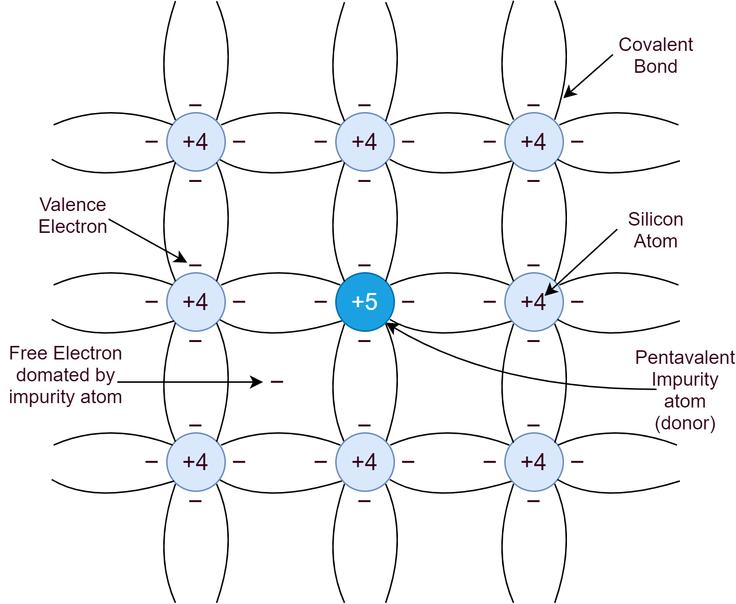
- Doping introduces carriers into the gap region: donors add electrons near the conduction band, acceptors add holes near the valence band
- Effective mass differs from the free electron mass and varies between materials. In GaAs, the electron effective mass is only , which gives high mobility
- Carrier concentration in metals is fixed ( cm), while in semiconductors it's tunable over many orders of magnitude through doping and temperature
Nanostructures and quantum confinement
When a structure's dimensions shrink to the scale of the electron's de Broglie wavelength (typically a few nanometers in semiconductors), confinement quantizes the energy levels and reshapes the density of states:
- Quantum wells (2D confinement in one direction): step-like density of states
- Quantum wires (1D): density of states with van Hove singularities ( divergences)
- Quantum dots (0D): fully discrete energy levels, like artificial atoms
This tunability is the basis for quantum dot lasers, single-electron transistors, and other nanoelectronic devices where controlling the electronic spectrum through geometry gives you design freedom that bulk materials can't offer.