🧶Inorganic Chemistry I Unit 14 Review
14.2 Characterization Techniques: XRD, SEM, and TEM
14.2 Characterization Techniques: XRD, SEM, and TEM
Unit & Topic Study Guides
Atomic Structure & Periodic Trends
Chemical Bonding Theories
Molecular Symmetry and Group Theory
Main Group Elements
Main Group Elements
Acid-Base Concepts in Inorganic Chem
Redox Reactions in Electrochemistry
Coordination Compounds: Structures & Isomers
Coordination Compounds: Bonding Theories
Coordination Compounds: Spectra & Magnetism
Organometallic Chemistry: Structures & Bonds
Organometallic Reactions and Catalysis
Solid-State Structures in Inorganic Chemistry
Inorganic Materials: Synthesis & Analysis
X-ray Diffraction (XRD)
Principles and Applications of XRD
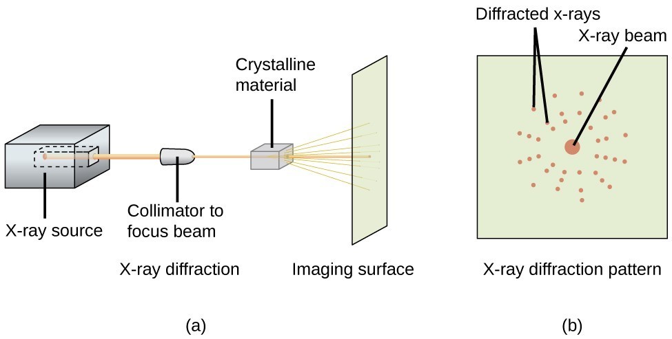
X-ray diffraction works by directing a beam of X-rays at a crystalline sample and measuring how those X-rays scatter off the regularly spaced planes of atoms. Because atoms in a crystal are arranged in a periodic lattice, the scattered X-rays interfere with each other, producing a characteristic diffraction pattern of peaks at specific angles. That pattern acts like a fingerprint for the crystal structure.
XRD is one of the most widely used techniques in inorganic chemistry and materials science. You can use it to:
- Identify unknown crystalline phases by matching diffraction patterns against reference databases (such as the ICDD PDF database)
- Determine unit cell parameters (, , , and angles , , )
- Estimate crystallite size and lattice strain from peak broadening (via the Scherrer equation)
- Quantify the relative amounts of different phases in a mixture (Rietveld refinement)
One limitation worth keeping in mind: XRD requires long-range periodic order to produce sharp diffraction peaks. Amorphous materials produce only broad, diffuse humps rather than distinct peaks, so XRD is primarily a tool for crystalline phases.
Bragg's Law and Diffraction Mechanics
Constructive interference of scattered X-rays only happens under specific geometric conditions. Bragg's Law captures those conditions:
where:
- = order of reflection (a positive integer: 1, 2, 3…)
- = wavelength of the incident X-rays (commonly Cu Kα, Å)
- = spacing between parallel planes of atoms (the interplanar distance)
- = angle between the incident beam and the crystal planes (the Bragg angle)
Here's how to think about it: X-rays reflecting off two adjacent planes travel slightly different path lengths. When that path difference equals exactly , the reflected waves add together (constructive interference), producing a peak in the diffraction pattern. When the condition isn't met, the waves cancel out through destructive interference.
In a typical XRD experiment, you vary by rotating the sample and detector. Each peak in the resulting plot of intensity vs. corresponds to a specific set of lattice planes with Miller indices and spacing . You can rearrange Bragg's Law to calculate from a measured peak position:
For a cubic system, the relationship between -spacing and the lattice parameter is:
This means that once you index the peaks (assign values), you can extract the unit cell dimensions directly from the diffraction pattern.
Types of XRD Techniques
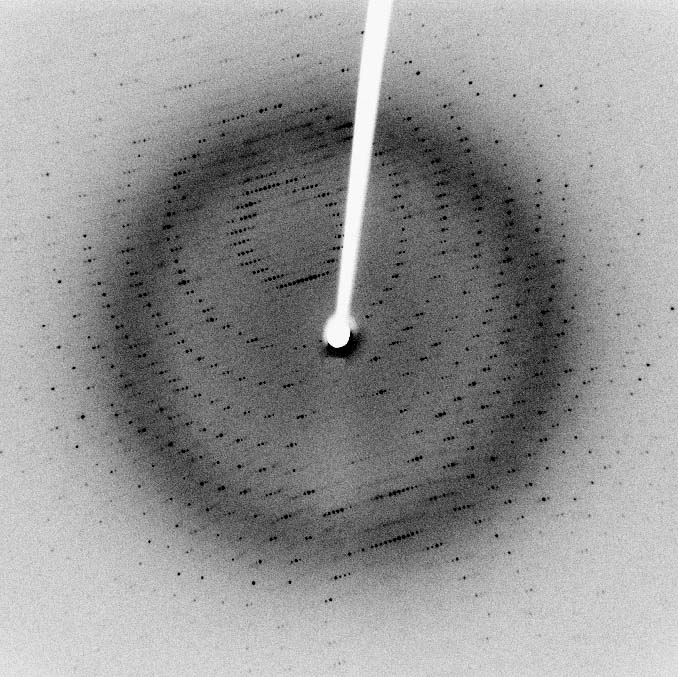
Powder XRD is the more common method for routine characterization. The sample is ground into a fine powder so that crystallites sit in every possible orientation. This ensures that for any given angle, some crystallites will satisfy Bragg's Law. The result is a pattern of peaks (historically recorded as concentric Debye-Scherrer rings on film, now typically as a vs. intensity plot from a diffractometer). Powder XRD is the go-to technique for phase identification, quantitative phase analysis, and determining unit cell dimensions.
Single-crystal XRD examines one well-formed crystal, typically at least ~0.1 mm in size. Because you can rotate the crystal systematically and measure diffraction in three dimensions, this technique yields far more detailed structural information. You can determine the full crystal structure: exact atomic positions, bond lengths, bond angles, and thermal displacement parameters. The trade-off is that it requires a crystal of sufficient size and quality, and data collection and refinement take considerably more time.
Electron Microscopy
Scanning Electron Microscopy (SEM)
SEM creates images by rastering a focused electron beam across the surface of a sample and collecting the signals generated at each point. It's the technique you reach for when you need to see surface morphology, particle shapes, grain boundaries, or fracture surfaces.
Two main types of signals carry different information:
- Secondary electrons (SE): Low-energy electrons (< 50 eV) knocked out of the sample surface. They're very sensitive to surface topography, so SE images look three-dimensional and show fine surface detail. Because of their low energy, only SE generated very near the surface escape, giving excellent surface sensitivity.
- Backscattered electrons (BSE): Higher-energy electrons that bounce back from deeper in the sample after elastic scattering off nuclei. Heavier elements scatter more electrons, so BSE images give compositional contrast: brighter regions contain higher- elements.
Typical SEM resolution falls in the 1–20 nm range, depending on the instrument, beam conditions, and sample. Magnification spans roughly 10× to 500,000×. One practical requirement: samples must be electrically conductive to avoid charge buildup that distorts the image. Non-conductive samples (ceramics, polymers) are usually sputter-coated with a thin layer of gold, platinum, or carbon before imaging. Alternatively, environmental or variable-pressure SEM modes allow imaging of non-conductive samples without coating by using a low-vacuum gas environment to dissipate charge.
Transmission Electron Microscopy (TEM)
TEM pushes resolution much further by transmitting electrons through an ultra-thin specimen rather than scanning across its surface. This gives you access to internal microstructure at extremely high resolution.
- Standard TEM resolution reaches below 1 Å in modern aberration-corrected instruments, enough to resolve individual atomic columns.
- Samples must be very thin, typically less than 100 nm, so that enough electrons pass through to form an image.
- Bright-field (BF) imaging uses the directly transmitted beam. Thicker or denser regions appear darker because they scatter more electrons out of the beam. This gives mass-thickness contrast.
- Dark-field (DF) imaging selects a specific diffracted beam instead by tilting the beam or displacing the objective aperture. Only regions diffracting at that particular angle appear bright, which is useful for highlighting grains of a specific crystallographic orientation or identifying precipitate phases.
- High-resolution TEM (HRTEM) uses phase contrast from multiple interfering beams to produce lattice fringe images, directly revealing the arrangement of atomic planes. The spacings you measure in these images correspond to -spacings of the crystal, connecting TEM directly back to the information you get from XRD.
TEM magnification can exceed 1,000,000×, but the real power is in the combination of imaging with diffraction and spectroscopy (see below).
Advanced Electron Microscopy Techniques
Both SEM and TEM can be paired with analytical techniques that go beyond imaging:
Electron diffraction produces patterns analogous to XRD but from a much smaller region of the sample. In TEM, Selected Area Electron Diffraction (SAED) lets you place an aperture over a specific area (down to a few hundred nm) and collect its diffraction pattern. For a single-crystal grain, SAED produces a pattern of discrete spots whose geometry reflects the reciprocal lattice of that crystal. For a polycrystalline region, you'll see rings similar to a powder XRD pattern. This tells you the crystal structure and orientation of that particular grain or particle, which is something powder XRD can't do on a local scale.
Energy-dispersive X-ray spectroscopy (EDS/EDX) detects the characteristic X-rays emitted when the electron beam knocks out inner-shell electrons from atoms in the sample. Each element produces X-rays at specific energies, so EDS gives you elemental composition. You can collect a single spectrum from a point, a line scan across a feature, or a full elemental map of the field of view. EDS works in both SEM and TEM, making it one of the most versatile analytical add-ons. Note that EDS is generally less sensitive to light elements (, i.e., lighter than Na), though modern detectors have improved this.
Sample Preparation and Microscope Operation
Sample preparation is often the most challenging part of electron microscopy, especially for TEM.
- SEM preparation is relatively straightforward. Conductive samples can often be mounted and imaged directly. Non-conductive samples need a thin conductive coating. Biological or hydrated samples require drying or fixation to survive the vacuum.
- TEM preparation demands that the sample be thinned to electron transparency (< 100 nm). Common methods include:
- Ultramicrotomy: Cutting ultra-thin slices with a diamond knife (common for softer materials and polymers)
- Ion milling: Using an argon ion beam to gradually thin a pre-prepared disc (common for ceramics, minerals, and hard inorganic materials)
- Focused Ion Beam (FIB): A gallium ion beam precisely cuts and thins a specific region of interest. FIB is especially valuable for preparing cross-sections from bulk samples or targeting specific features like grain boundaries or interfaces. One caveat: FIB can introduce surface amorphization and gallium implantation, which may need to be accounted for.
Resolution in both instruments depends on the electron source (field-emission guns give the best coherence and brightness), the quality of the electromagnetic lenses, and how well the sample is prepared. Vibration, stray magnetic fields, and contamination can all degrade performance.
Quick comparison: XRD gives you bulk-averaged crystal structure data from a large volume of material. SEM shows you surface morphology and composition with nm-scale resolution. TEM reveals internal structure down to the atomic level but requires the most demanding sample preparation. In practice, these techniques are complementary: you'll often use two or all three on the same material to build a complete picture.