Semiconductor devices are the building blocks of modern electronics, utilizing the unique properties of materials like and . These devices, including transistors and diodes, form the foundation of integrated circuits that power our digital world.

This topic explores various semiconductor devices, their underlying physics, and fabrication techniques. From basic p-n junctions to advanced quantum well structures, we'll examine how these devices work and their applications in electronics and optoelectronics.

Types of semiconductor devices

  • Semiconductor devices are electronic components that exploit the electrical properties of semiconductor materials (silicon, , gallium arsenide)
  • They form the foundation of modern electronics, enabling the development of transistors, diodes, and integrated circuits
  • Semiconductor devices have revolutionized various fields, including computing, telecommunications, and consumer electronics

Semiconductor materials

Elemental semiconductors

Top images from around the web for Elemental semiconductors
  • Elemental semiconductors consist of a single element from group IV of the periodic table (silicon, germanium)
  • Silicon is the most widely used elemental semiconductor due to its abundance, low cost, and favorable electrical properties
  • Germanium was used in early semiconductor devices but has been largely replaced by silicon

Compound semiconductors

  • Compound semiconductors are formed by combining elements from groups III and V (gallium arsenide, indium phosphide) or groups II and VI (cadmium telluride, zinc selenide) of the periodic table
  • They offer unique properties such as higher electron mobility, wider bandgaps, and better optical performance compared to elemental semiconductors
  • Compound semiconductors find applications in high-frequency electronics, optoelectronics, and photovoltaics

Energy bands in semiconductors

Valence and conduction bands

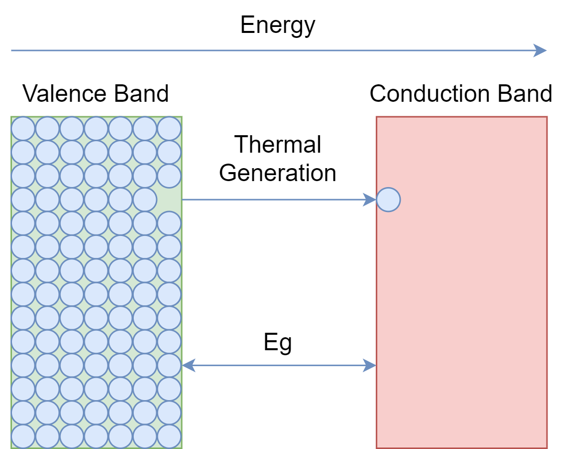
  • In semiconductors, the valence band is the highest occupied energy band at absolute zero temperature, while the conduction band is the lowest unoccupied energy band
  • Electrons in the valence band are bound to the atoms and do not contribute to electrical conduction
  • Electrons in the conduction band are free to move and participate in electrical conduction

Band gap and Fermi level

  • The is the energy difference between the top of the valence band and the bottom of the conduction band
  • The Fermi level represents the energy level at which the probability of an electron occupying a state is 50%
  • In intrinsic semiconductors, the Fermi level lies approximately in the middle of the band gap
  • can shift the Fermi level towards the conduction band (n-type) or valence band (p-type)

Charge carriers in semiconductors

Electrons and holes

  • Electrons are negatively charged particles that can move freely in the conduction band and contribute to electrical conduction
  • Holes are the absence of electrons in the valence band and behave as positively charged particles
  • Both electrons and holes can participate in electrical conduction in semiconductors

Intrinsic vs extrinsic semiconductors

  • Intrinsic semiconductors are pure semiconductors without any intentional doping
  • In intrinsic semiconductors, the number of electrons in the conduction band equals the number of holes in the valence band
  • Extrinsic semiconductors are doped with impurities to increase the concentration of either electrons (n-type) or holes (p-type)
  • Doping allows for the control of electrical properties and the creation of semiconductor devices

Doping of semiconductors

n-type doping

  • involves introducing impurities (dopants) with an excess of valence electrons (phosphorus, arsenic) into the semiconductor material
  • The extra electrons from the dopants occupy energy levels near the conduction band, making it easier for them to be excited into the conduction band
  • n-type semiconductors have a higher concentration of electrons compared to holes

p-type doping

  • involves introducing impurities (dopants) with a deficiency of valence electrons (boron, gallium) into the semiconductor material
  • The missing electrons create holes in the valence band, which can accept electrons from neighboring atoms
  • p-type semiconductors have a higher concentration of holes compared to electrons

p-n junctions

Built-in potential

  • When a p-type and an n-type semiconductor are brought into contact, a p-n junction is formed
  • Due to the concentration gradient, electrons diffuse from the n-type region to the p-type region, and holes diffuse in the opposite direction
  • This creates a (VbiV_{bi}) across the junction, which opposes further diffusion of charge carriers

Depletion region

  • The diffusion of charge carriers leaves behind immobile ionized dopant atoms near the p-n junction, creating a region depleted of free charge carriers called the
  • The depletion region has a high resistance and acts as a barrier to the flow of charge carriers
  • The width of the depletion region depends on the doping concentrations and the applied voltage

Forward vs reverse bias

  • occurs when a positive voltage is applied to the p-type region and a negative voltage to the n-type region, reducing the built-in potential and allowing current to flow through the p-n junction
  • occurs when a negative voltage is applied to the p-type region and a positive voltage to the n-type region, increasing the built-in potential and preventing current flow
  • The behavior of a p-n junction under forward and reverse bias forms the basis for the operation of diodes and other semiconductor devices

Diodes

Ideal vs real diodes

  • An allows current to flow in the forward direction (forward bias) with zero resistance and blocks current flow in the reverse direction (reverse bias) with infinite resistance
  • Real diodes have a small (VfV_f) in the forward bias condition, typically 0.6-0.7 V for silicon diodes and 0.2-0.3 V for germanium diodes
  • Real diodes also have a small leakage current in the reverse bias condition, known as the (IsI_s)

Current-voltage characteristics

  • The current-voltage (I-V) characteristics of a describe its behavior under different bias conditions
  • In the forward bias region, the current increases exponentially with the applied voltage according to the Shockley diode equation: I=Is(eqV/kT1)I = I_s(e^{qV/kT} - 1)
  • In the reverse bias region, the current remains close to the reverse saturation current until the reverse breakdown voltage is reached, at which point the current increases rapidly

Diode applications

  • Rectification: Diodes are used to convert alternating current (AC) to direct current (DC) by allowing current to flow only in one direction (half-wave rectification, full-wave rectification)
  • Voltage regulation: Zener diodes are used to maintain a constant voltage across a load by operating in the reverse breakdown region
  • Overvoltage protection: Diodes can be used to protect circuits from voltage spikes by limiting the voltage across sensitive components
  • Logic gates: Diodes are used in the implementation of logic gates (AND, OR) in diode-resistor logic (DRL) and diode- logic (DTL)

Bipolar junction transistors (BJTs)

npn vs pnp transistors

  • BJTs are three-terminal devices consisting of three differently doped semiconductor regions: emitter, base, and collector
  • npn transistors have a thin p-type base region sandwiched between two n-type regions (emitter and collector)
  • pnp transistors have a thin n-type base region sandwiched between two p-type regions (emitter and collector)
  • The type of transistor (npn or pnp) determines the direction of current flow and the polarity of the voltages applied to the terminals

Transistor operation and configurations

  • BJTs operate by controlling the current flow between the emitter and the collector through a small current injected into the base
  • The three main configurations of BJTs are common emitter (CE), common base (CB), and common collector (CC), each with different input and output characteristics
  • In the CE configuration, a small change in the base current results in a large change in the collector current, making it suitable for amplification and switching applications

Current gain and amplification

  • The (β\beta) of a BJT is the ratio of the collector current (ICI_C) to the base current (IBI_B): β=IC/IB\beta = I_C/I_B
  • BJTs can achieve high current gains, typically in the range of 50 to 200, enabling them to amplify small input signals
  • The voltage gain (AVA_V) of a BJT amplifier is the product of the current gain and the ratio of the collector resistor (RCR_C) to the emitter resistor (RER_E): AV=β(RC/RE)A_V = \beta (R_C/R_E)

Field-effect transistors (FETs)

JFET vs MOSFET

  • FETs are three-terminal devices that control the current flow through a semiconductor channel by applying an electric field
  • Junction FETs (JFETs) have a reverse-biased p-n junction to control the channel conductivity, while metal-oxide-semiconductor FETs (MOSFETs) use an insulated gate electrode
  • JFETs are depletion-mode devices, meaning they are normally on and require a reverse bias to turn off, while MOSFETs can be either depletion-mode or enhancement-mode (normally off)

Gate, source, and drain

  • The three terminals of a FET are the gate, source, and drain
  • The gate controls the channel conductivity by applying an electric field, the source is the terminal through which carriers enter the channel, and the drain is the terminal through which carriers leave the channel
  • In n-channel FETs, electrons are the majority carriers, while in p-channel FETs, holes are the majority carriers

Transistor operation and characteristics

  • FETs operate by modulating the channel conductivity through the application of a
  • The gate voltage controls the depletion region width in JFETs or the inversion layer thickness in MOSFETs, which in turn affects the channel resistance and the
  • The output characteristics of FETs show the relationship between the drain current (IDI_D) and the (VDSV_{DS}) for different gate-source voltages (VGSV_{GS})
  • The transfer characteristics of FETs show the relationship between the drain current (IDI_D) and the gate-source voltage (VGSV_{GS}) for a fixed drain-source voltage (VDSV_{DS})

Semiconductor device fabrication

Photolithography and etching

  • is a process used to transfer patterns from a photomask to the surface of a semiconductor wafer
  • The wafer is coated with a light-sensitive material called photoresist, which is then exposed to light through the photomask
  • The exposed regions of the photoresist are selectively removed (positive photoresist) or retained (negative photoresist) during development
  • is used to remove the uncovered regions of the semiconductor material or other layers, transferring the pattern from the photoresist to the wafer

Diffusion and ion implantation

  • Diffusion is a process used to introduce dopants into the semiconductor material by exposing the wafer to a high-temperature environment containing the dopant atoms
  • The dopant atoms diffuse into the semiconductor material, creating regions with different electrical properties (n-type or p-type)
  • is an alternative doping method that involves accelerating dopant ions and directing them towards the wafer surface
  • Ion implantation offers better control over the dopant concentration and depth profile compared to diffusion

Metallization and packaging

  • is the process of depositing metal layers on the semiconductor wafer to create electrical connections and contacts
  • Metal layers (aluminum, copper) are deposited using physical vapor deposition (PVD) or (CVD) techniques
  • The metal layers are patterned using photolithography and etching to form the desired interconnect structures
  • involves encapsulating the semiconductor device in a protective package (plastic, ceramic) and connecting it to external leads or pins for integration into electronic circuits

Advanced semiconductor devices

Thyristors and IGBTs

  • Thyristors are four-layer (pnpn) semiconductor devices that exhibit bistable switching characteristics, making them suitable for high-power applications (power control, switching)
  • Insulated-gate bipolar transistors () combine the high input impedance and voltage control of MOSFETs with the low on-state resistance and high current capability of BJTs
  • IGBTs are widely used in power electronics applications, such as motor drives, inverters, and switch-mode power supplies

Optoelectronic devices

  • convert electrical signals to optical signals (, ) or optical signals to electrical signals (, solar cells)
  • Light-emitting diodes () are p-n junction devices that emit light when forward-biased, finding applications in lighting, displays, and optical communication
  • Laser diodes are similar to LEDs but produce coherent, monochromatic light through stimulated emission, enabling applications in fiber-optic communication, barcode scanners, and laser pointers

Quantum well and superlattice devices

  • are based on thin layers of semiconductor materials with different bandgaps, creating potential wells that confine charge carriers in one dimension
  • Quantum wells exhibit unique electronic and optical properties, such as enhanced and discrete energy levels, making them suitable for high-speed electronics and optoelectronics
  • consist of alternating layers of two different semiconductor materials, creating a periodic potential that affects the electronic and optical properties
  • Superlattices find applications in infrared detectors, terahertz devices, and quantum cascade lasers

Key Terms to Review (57)

Band Gap: The band gap is the energy difference between the top of the valence band and the bottom of the conduction band in a solid material, determining its electrical conductivity. This energy range is crucial for understanding how materials interact with electrons, which is essential when discussing crystal structures, electron behavior, and how phonons affect these dynamics.
Bipolar Junction Transistor: A bipolar junction transistor (BJT) is a type of semiconductor device that can amplify or switch electronic signals and electrical power. It consists of three layers of doped semiconductor material, forming two p-n junctions, which are classified as either NPN or PNP based on the arrangement of the n-type and p-type materials. BJTs are widely used in electronic circuits for amplification and switching applications, making them fundamental components in modern electronics.
Built-in Potential: Built-in potential refers to the electric potential that develops across the junction of a semiconductor device when two different types of semiconductor materials, typically p-type and n-type, are brought into contact. This potential barrier is crucial for the operation of devices such as diodes and transistors, as it helps to establish the conditions for charge carrier movement and recombination, ultimately influencing the current flow within the device.
Carrier Mobility: Carrier mobility is a measure of how quickly charge carriers, such as electrons and holes, can move through a semiconductor material when subjected to an electric field. This property significantly affects the performance of semiconductor devices, influencing parameters like conductivity, switching speeds, and overall efficiency. Higher carrier mobility results in better electrical performance, making it a crucial factor in the design and application of various semiconductor technologies.
Chemical Vapor Deposition: Chemical vapor deposition (CVD) is a process used to produce thin films and coatings by depositing material from a vapor phase onto a substrate through chemical reactions. This technique is vital for creating high-purity and uniform materials, making it essential in the fabrication of various advanced technologies, including electronic components, nanomaterials, and novel two-dimensional structures.
Common Base Configuration: The common base configuration is a type of transistor amplifier circuit where the base terminal is common to both the input and output. This configuration provides a high-frequency response and is often used in applications where voltage gain and low input impedance are required. The common base setup is typically less common than other configurations, such as common emitter or common collector, but it offers unique advantages for specific use cases.
Common collector configuration: The common collector configuration is a type of transistor amplifier circuit where the collector terminal is common to both the input and output signals. This configuration is often used for voltage buffering, as it provides high input impedance and low output impedance, making it ideal for interfacing different circuit stages without signal loss or loading effects.
Common emitter configuration: The common emitter configuration is a widely used transistor amplifier setup where the emitter terminal is common to both the input and output circuits. This configuration is significant due to its ability to provide voltage gain and phase inversion, making it essential in amplification applications within semiconductor devices. The common emitter arrangement enhances signal processing, allowing for effective amplification in various electronic circuits.
Current Gain: Current gain refers to the ratio of output current to input current in a semiconductor device, especially transistors. This parameter is crucial for understanding how effectively a transistor can amplify signals, as it indicates the ability of the device to increase current from the input to the output, impacting performance in various applications such as amplifiers and switches.
Current-voltage characteristics: Current-voltage characteristics describe the relationship between the electric current flowing through a semiconductor device and the voltage across it. This relationship is crucial in understanding how semiconductor devices operate, as it helps to identify their behavior under different electrical conditions, enabling engineers to design and utilize these devices effectively in electronic applications.
Depletion Region: The depletion region is a zone in a semiconductor device, particularly in p-n junctions, where mobile charge carriers (electrons and holes) are depleted, resulting in an electric field that forms a potential barrier. This area plays a crucial role in the operation of semiconductor devices, affecting their ability to conduct current and their overall electrical properties.
Diffusion: Diffusion is the process by which particles spread from areas of high concentration to areas of low concentration, driven by random thermal motion. This phenomenon is crucial in various materials, affecting how substances move through solids, including the performance of semiconductor devices, the behavior of defects in materials, and the formation and migration of point defects within crystal lattices.
Diode: A diode is a semiconductor device that allows current to flow in one direction while blocking it in the opposite direction. This property makes diodes essential components in various electronic applications, such as rectifiers, signal modulators, and voltage regulators. Their behavior is closely linked to the characteristics of intrinsic and extrinsic semiconductors, as well as the broader category of semiconductor devices.
Doping: Doping refers to the intentional introduction of impurities into a semiconductor material to modify its electrical properties. This process creates either n-type or p-type semiconductors by adding donor or acceptor atoms, respectively, which alters the energy bands and bandgaps, leading to significant changes in conductivity and electronic behavior.
Drain Current: Drain current refers to the flow of electric current from the drain terminal of a field-effect transistor (FET) to the source terminal when a voltage is applied. This current is crucial in the operation of semiconductor devices, as it allows for the modulation of electronic signals and plays a vital role in the functioning of various electronic components.
Drain Terminal: The drain terminal is a key component in field-effect transistors (FETs) that allows current to exit the device. This terminal plays a crucial role in controlling the flow of electrical current through the transistor, enabling it to function as an amplifier or a switch. Its operation is closely linked with the gate and source terminals, which together regulate the conductivity of the channel formed within the semiconductor material.
Drain-Source Voltage: Drain-source voltage (V_DS) refers to the voltage difference between the drain and source terminals of a field-effect transistor (FET). This voltage is crucial for controlling the current flow through the device, and its value determines whether the transistor is in an 'on' or 'off' state, significantly impacting the operation of various semiconductor devices.
Etching: Etching is a process used in semiconductor manufacturing to selectively remove layers from the surface of a material, typically silicon, by using chemical or physical means. This technique is essential for creating intricate patterns and structures on semiconductor devices, which are crucial for their functionality. Etching allows for the precise definition of features necessary for components like transistors and capacitors in integrated circuits.
Field-effect transistor: A field-effect transistor (FET) is a type of transistor that uses an electric field to control the flow of current. This device allows for efficient signal amplification and switching, making it essential in various electronic applications. FETs are crucial in semiconductor devices due to their high input impedance and low power consumption, which help in the design of integrated circuits and other electronic components.
Forward bias: Forward bias is a condition in semiconductor devices where the p-type material is connected to the positive terminal of a voltage source and the n-type material is connected to the negative terminal. This arrangement reduces the potential barrier at the p-n junction, allowing current to flow easily across it. The result of forward bias is that charge carriers are injected into the depletion region, leading to increased conductivity and enabling the device to operate as intended.
Forward voltage drop: Forward voltage drop refers to the voltage that is lost when current flows through a semiconductor device, such as a diode or transistor, in the forward bias direction. This voltage drop occurs due to the internal resistance and the energy required to move charge carriers across the junction of the semiconductor. Understanding forward voltage drop is essential for predicting how devices will behave in circuits, especially regarding power consumption and efficiency.
Gallium Arsenide: Gallium arsenide (GaAs) is a compound semiconductor material made from gallium and arsenic elements. It is known for its high electron mobility and direct bandgap, making it highly effective for use in high-frequency and optoelectronic devices, such as lasers and solar cells. The unique properties of GaAs allow it to outperform traditional silicon-based semiconductors in specific applications, especially in telecommunications and advanced electronics.
Gate voltage: Gate voltage refers to the electrical potential applied to the gate terminal of a semiconductor device, particularly in field-effect transistors (FETs). This voltage is crucial because it controls the conductivity of the channel between the source and drain terminals, essentially acting as a switch that determines whether the device is on or off. The level of gate voltage influences how many charge carriers are present in the channel, directly affecting the overall performance and behavior of the semiconductor device.
Germanium: Germanium is a chemical element with the symbol Ge and atomic number 32. It is a key semiconductor material used in various electronic devices, playing a vital role in the development of transistors and diodes. Its properties allow for efficient electron movement, making it essential in modern technology, particularly in semiconductor devices.
Ideal diode: An ideal diode is a theoretical semiconductor device that allows current to flow freely in one direction while completely blocking current in the reverse direction. This concept is crucial for understanding how diodes function in electronic circuits, providing perfect rectification without any voltage drop or leakage current.
IGBTs: IGBTs, or Insulated Gate Bipolar Transistors, are semiconductor devices that combine the characteristics of both MOSFETs and bipolar transistors, making them ideal for high-efficiency and high-voltage applications. They are widely used in power electronics due to their ability to control large amounts of current while maintaining a low on-state voltage drop. This unique combination allows IGBTs to operate efficiently in various applications such as motor drives, renewable energy systems, and power inverters.
Ion implantation: Ion implantation is a process used to introduce impurities or dopants into a semiconductor material by bombarding it with high-energy ions. This technique is crucial in the fabrication of semiconductor devices as it allows for precise control over the concentration and distribution of dopants, enabling the modification of electrical properties necessary for creating p-n junctions and other electronic components.
Jack Kilby: Jack Kilby was an American engineer and inventor, best known for his pioneering work in the development of the integrated circuit in the 1950s. His contributions revolutionized the field of electronics, laying the foundation for modern semiconductor devices and enabling the miniaturization of electronic components, which transformed technology as we know it.
JFET: A Junction Field Effect Transistor (JFET) is a type of transistor that utilizes an electric field to control the flow of current. It is a key component in semiconductor devices, where it operates as a voltage-controlled resistor. JFETs are widely used in amplifiers, switches, and digital circuits due to their high input impedance and low noise characteristics.
Laser diodes: Laser diodes are semiconductor devices that convert electrical energy into coherent light through the process of stimulated emission. They are crucial components in various applications, including telecommunications, barcode scanners, and laser printers, due to their efficiency and compact size.
LEDs: Light Emitting Diodes (LEDs) are semiconductor devices that emit light when an electric current passes through them. They are based on the principle of electroluminescence, where electrons recombine with holes in a semiconductor material, releasing energy in the form of photons. This process is closely tied to the behavior of p-n junctions, the properties of semiconductors, and the impact of quantum confinement in nanostructures.
Light-emitting diodes: Light-emitting diodes (LEDs) are semiconductor devices that emit light when an electric current passes through them. They are widely used for various applications, including lighting, displays, and indicators due to their energy efficiency and long lifespan. The operation of LEDs is based on the principle of electroluminescence, where the recombination of electrons and holes in the semiconductor material releases energy in the form of light.
Metallization: Metallization refers to the process of depositing a thin layer of metal onto a surface to create a conductive pathway, essential in the fabrication of semiconductor devices. This technique is crucial for establishing electrical connections between different components within these devices, ensuring their functionality and efficiency. By enabling the integration of various materials, metallization plays a key role in enhancing device performance and reliability.
MOSFET: A MOSFET, or Metal-Oxide-Semiconductor Field-Effect Transistor, is a type of transistor used for switching and amplifying electronic signals in various devices. It is a key component in modern electronics, allowing for the control of electrical current with an applied voltage. The structure of a MOSFET includes a gate, drain, and source, making it essential for both digital and analog applications in semiconductor devices.
MOSFET Operation: MOSFET operation refers to the functioning of the Metal-Oxide-Semiconductor Field-Effect Transistor, a key component in modern electronics. This device operates by controlling the flow of current through a semiconductor channel with an electric field, enabling various applications in amplification and switching. The unique structure of MOSFETs, including gate, source, and drain terminals, plays a critical role in its efficiency and performance in semiconductor devices.
N-type doping: N-type doping is the process of adding impurities to a semiconductor material, typically silicon, to increase the number of free electrons, thereby enhancing its electrical conductivity. This is achieved by introducing donor atoms that have more valence electrons than the semiconductor itself, which creates additional charge carriers that contribute to electrical current. N-type doping plays a crucial role in the functionality of various semiconductor devices, including transistors and diodes.
Npn transistor: An npn transistor is a type of bipolar junction transistor that consists of three layers: two n-type semiconductor materials (negative) and one p-type semiconductor material (positive) in between. This configuration allows the transistor to amplify current and switch electronic signals, making it crucial in various semiconductor devices used for controlling and processing signals.
Optoelectronic devices: Optoelectronic devices are components that involve the interaction between light and electrical signals, enabling the conversion of electrical energy into optical energy and vice versa. These devices are essential in various applications, including communication, sensing, and imaging technologies, and rely on semiconductor materials to function effectively. The ability to manipulate light at the semiconductor level has led to significant advancements in technology, influencing everything from telecommunications to consumer electronics.
P-type doping: p-type doping is the process of adding specific impurities, known as acceptors, to a semiconductor material to create an abundance of holes, which are the absence of electrons, leading to a positive charge carrier. This technique is crucial for enhancing the electrical conductivity of semiconductors by allowing them to facilitate charge flow more efficiently. p-type materials are formed when elements from group III of the periodic table, like boron or aluminum, are introduced into a silicon lattice, effectively creating an excess of holes that act as charge carriers.
Packaging: Packaging refers to the process of enclosing semiconductor devices in protective materials and structures to ensure their integrity, functionality, and reliability. It plays a crucial role in the performance and lifespan of semiconductor devices by providing mechanical support, protecting against environmental factors, and facilitating electrical connections. Proper packaging techniques also enable efficient thermal management and contribute to the overall manufacturability of electronic systems.
Photodiodes: Photodiodes are semiconductor devices that convert light into electrical current. They are designed to be sensitive to light and operate by the principle of the photoelectric effect, where incident photons generate electron-hole pairs in the semiconductor material, resulting in a measurable electrical signal. Photodiodes are widely used in various applications such as optical communication, light detection, and imaging systems.
Photolithography: Photolithography is a process used in microfabrication to transfer geometric patterns onto a substrate, typically a silicon wafer, using light. This technique is essential for creating intricate circuit patterns in semiconductor devices and is key to the manufacturing of integrated circuits and microelectromechanical systems (MEMS). It involves coating the substrate with a photosensitive material, exposing it to light through a mask, and developing the exposed areas to create the desired pattern.
Photovoltaic cells: Photovoltaic cells are semiconductor devices that convert light energy directly into electrical energy through the photovoltaic effect. These cells are crucial for solar power applications, as they enable the capture and conversion of sunlight into usable electricity, which plays a key role in renewable energy technologies and sustainable power solutions.
Pn junction: A pn junction is a boundary or interface between p-type and n-type semiconductor materials, crucial for the operation of various semiconductor devices. This junction is formed when p-type material, which has an abundance of holes (positive charge carriers), is placed in contact with n-type material, which has an excess of electrons (negative charge carriers). The interaction at this junction creates a depletion region and establishes an electric field that plays a key role in the behavior of diodes and transistors.
Pnp transistor: A pnp transistor is a type of bipolar junction transistor that consists of three layers of semiconductor material, specifically arranged with p-type material on the outer layers and n-type material in the center. This configuration allows for the control of current flow between the layers, enabling amplification and switching applications in various electronic circuits.
Quantum well devices: Quantum well devices are semiconductor structures that confine carriers (electrons and holes) in a thin layer, creating potential wells that restrict their movement in one dimension. This unique confinement leads to quantized energy levels, which enables various electronic and optoelectronic applications such as lasers, photodetectors, and high-electron-mobility transistors. The ability to manipulate electronic properties at the nanoscale makes quantum well devices essential for modern technology.
Real Diode: A real diode is a semiconductor device that allows current to flow in one direction while blocking it in the opposite direction, exhibiting non-ideal behaviors due to various factors like series resistance and junction capacitance. This means that while it serves the fundamental purpose of rectification, the actual performance deviates from the ideal characteristics due to physical limitations. Understanding these non-ideal properties is crucial for accurately modeling and applying diodes in electronic circuits.
Recombination: Recombination refers to the process where an electron and a hole recombine, resulting in the release of energy, typically in the form of a photon. This phenomenon is crucial in semiconductor devices, as it influences the efficiency and performance of various electronic components by determining how charge carriers behave within the material.
Reverse bias: Reverse bias refers to the condition in which a voltage is applied across a p-n junction in such a way that it widens the depletion region and prevents current flow. This condition is critical for the operation of various semiconductor devices, where controlling current flow is essential for their functionality. Understanding reverse bias is fundamental when discussing how p-n junctions behave under different voltage conditions and how this affects the performance of semiconductor devices like diodes and transistors.
Reverse saturation current: Reverse saturation current is the small amount of current that flows through a semiconductor diode when it is reverse-biased, meaning the voltage across the diode is applied in the opposite direction to its conductive path. This current is primarily due to the thermally generated minority carriers in the depletion region of the diode. It plays a crucial role in determining the behavior of diodes and is an important factor in applications like photodiodes and solar cells.
Robert Noyce: Robert Noyce was an American physicist and co-founder of Intel Corporation, known for his pivotal role in the development of the integrated circuit. His invention revolutionized semiconductor technology and laid the groundwork for modern electronics, greatly influencing the design and functionality of semiconductor devices.
Silicon: Silicon is a chemical element with the symbol Si and atomic number 14, renowned for its semiconductor properties that make it essential in the development of electronic devices. This element is abundant in the Earth's crust and is crucial in forming various materials, including silicon dioxide and silicates. Its ability to conduct electricity under certain conditions while insulating under others makes it a key player in modern technology, particularly in the fabrication of integrated circuits and solar cells.
Source terminal: The source terminal is a critical component in semiconductor devices, acting as the electrode through which carriers enter a device, such as a transistor. This terminal is essential for the operation of devices like MOSFETs and JFETs, where it establishes the flow of charge carriers into the channel, influencing the overall conductivity and switching behavior of the device. Understanding the role of the source terminal is vital for grasping how these semiconductor devices function in various electronic applications.
Superlattice devices: Superlattice devices are advanced semiconductor structures composed of alternating layers of two or more materials, each just a few nanometers thick. These structures enable the manipulation of electronic and optical properties by creating unique band structures, which are critical for applications in high-performance electronics and optoelectronics. The quantum effects arising from the layered materials lead to enhanced functionalities, such as improved electron mobility and novel light emission characteristics.
Threshold Voltage: Threshold voltage is the minimum gate-to-source voltage needed to create a conducting path between the source and drain terminals of a field-effect transistor (FET). This concept is essential in semiconductor devices because it determines when a transistor switches from its off state to its on state, influencing the device's overall performance and efficiency in electronic circuits.
Thyristor: A thyristor is a four-layer semiconductor device that acts as a switch, allowing current to flow when triggered and continuing to conduct until the current drops below a certain level. Thyristors are widely used in power control applications, including light dimmers, motor speed controls, and pressure control systems. They can handle high voltages and currents, making them ideal for industrial applications.
Transistor: A transistor is a semiconductor device that can amplify or switch electronic signals and electrical power. This crucial component is built from materials like silicon and can be classified into different types, such as bipolar junction transistors (BJTs) and field-effect transistors (FETs). Understanding how transistors operate is essential because they form the building blocks of modern electronic devices, including computers, radios, and smartphones.
© 2024 Fiveable Inc. All rights reserved.
AP® and SAT® are trademarks registered by the College Board, which is not affiliated with, and does not endorse this website.