Digital circuits fall into two categories: combinational and sequential. Combinational circuits produce outputs based solely on current inputs. Sequential circuits have memory, so their outputs depend on both current inputs and past states. Understanding the difference is foundational to designing everything from simple adders to complex processors.
Combinational vs Sequential Circuits
Characteristics and Differences
Combinational circuits produce an output that depends only on the current input values. There's no memory involved. Feed in the same inputs, and you'll always get the same output.
Sequential circuits produce an output that depends on both the current inputs and the circuit's stored state. Because they have memory elements, the same inputs can produce different outputs depending on what happened previously.
A few key distinctions:
- Combinational circuits are memoryless and don't require a clock signal
- Sequential circuits have memory and typically use a clock signal to synchronize when state changes happen
- Combinational circuits are simpler to design and analyze; sequential circuits enable more complex behavior like counting and storing data
Examples
- Combinational: adders, decoders, multiplexers, encoders
- Sequential: flip-flops, counters, shift registers, finite state machines
Design of Combinational Circuits
Logic Gates and Boolean Algebra
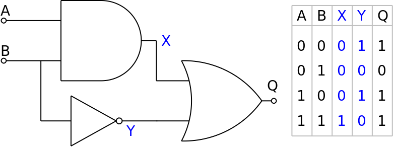
Combinational circuits are built from basic logic gates: AND, OR, NOT, NAND, NOR, and XOR. Each gate performs a logical operation on binary inputs and produces a binary output.
Boolean algebra is the math system used to describe and simplify these logical operations. The core operators are:
- AND (written as ): output is 1 only when both inputs are 1
- OR (written as ): output is 1 when at least one input is 1
- NOT (written as ): flips the input
To simplify Boolean expressions and reduce the number of gates needed, you can use:
- Truth tables to list every possible input/output combination
- Karnaugh maps (K-maps) to visually group terms and find simpler expressions
- Standard forms like sum-of-products (SOP) and product-of-sums (POS) to structure expressions in a way that maps directly to gate implementations
Analysis and Verification
You can verify a combinational circuit by working through its Boolean expression for every input combination and checking it against the expected truth table.
Example: The Half Adder
A half adder adds two single-bit inputs ( and ) and produces two outputs:
- Sum: (XOR gate)
- Carry: (AND gate)
Its truth table confirms the design:
| Sum () | Carry () | ||
|---|---|---|---|
| 0 | 0 | 0 | 0 |
| 0 | 1 | 1 | 0 |
| 1 | 0 | 1 | 0 |
| 1 | 1 | 0 | 1 |
Notice that when both inputs are 1, the sum wraps to 0 and the carry becomes 1, just like in binary.
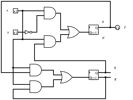
Flip-Flops and Latches in Sequential Circuits
Memory Elements
Flip-flops and latches are the basic building blocks that give sequential circuits their memory. Both store a single bit of data, but they differ in when they respond to input changes.
Latches are level-sensitive. They pass input changes through to the output whenever the enable signal is active (high or low, depending on design). As long as the enable is asserted, the latch is "transparent" and the output tracks the input.
- SR latch: has Set and Reset inputs. Setting drives output to 1; resetting drives it to 0.
- D latch: has a single Data input. The output follows D whenever enable is active.
Flip-flops are edge-triggered. They only update their output on a specific transition of the clock signal (either the rising edge or falling edge). This makes them more predictable in clocked systems because state changes happen at well-defined moments.
- D flip-flop: captures the value of D at the clock edge. The most commonly used type.
- JK flip-flop: like an SR flip-flop but with the added ability to toggle when both inputs are 1 (avoids the invalid state problem of SR).
- T flip-flop: toggles its output on each clock edge when the T input is 1.
Differences and Applications
The core difference: latches respond to input changes immediately while enabled, and flip-flops respond only at clock edges. This edge-triggered behavior is why flip-flops are preferred in synchronous designs, where you need all state changes to happen in lockstep with the clock.
Flip-flops and latches are combined to build larger structures:
- Registers: multiple D flip-flops grouped together to store multi-bit values (e.g., an 8-bit register stores one byte)
- Counters: flip-flops connected to cycle through binary states
- Finite state machines: flip-flops hold the current state while combinational logic determines the next state
Operation of Basic Sequential Circuits
Counters
Counters are sequential circuits that step through a sequence of binary values, incrementing (or decrementing) with each clock pulse. They're used for counting events, generating timing sequences, and dividing clock frequencies.
Asynchronous (ripple) counters chain flip-flops together so that the output of one flip-flop drives the clock input of the next. They're simple to build, but each flip-flop adds a small propagation delay, so the outputs don't all change at the same instant. This "ripple" effect limits how fast the counter can run.
Synchronous counters connect all flip-flops to the same clock signal. Additional combinational logic determines when each flip-flop should toggle. All outputs change simultaneously, making synchronous counters faster and more reliable at high speeds.
Example: A 4-bit binary ripple counter using T flip-flops counts from 0 to 15 ( to in binary). After reaching 15, it wraps back to 0 on the next clock pulse.
Shift Registers
Shift registers are chains of flip-flops where data moves one position on each clock pulse. They're useful for temporary data storage, introducing delays, and converting between serial and parallel data formats.
The four configurations are defined by how data enters and exits:
- SISO (Serial-In Serial-Out): data enters one bit at a time and exits one bit at a time
- SIPO (Serial-In Parallel-Out): data enters serially but all stored bits are available at once on the outputs
- PISO (Parallel-In Serial-Out): all bits load at once, then shift out one at a time
- PIPO (Parallel-In Parallel-Out): all bits load and are read simultaneously (acts more like a register with parallel access)
Two special shift register variants worth knowing:
- Ring counter: a shift register where the output of the last flip-flop feeds back to the first. A single 1 circulates through the chain. A 4-bit ring counter produces the repeating sequence: .
- Johnson counter: similar to a ring counter, but the inverted output of the last flip-flop feeds back. This produces twice as many unique states as a ring counter (a 4-bit Johnson counter has 8 unique states instead of 4).